••
Huawei Targets 1.4-nm Chip Breakthrough Within Five Years to Counter U.S. Sanctions
•3 min read•4 sources
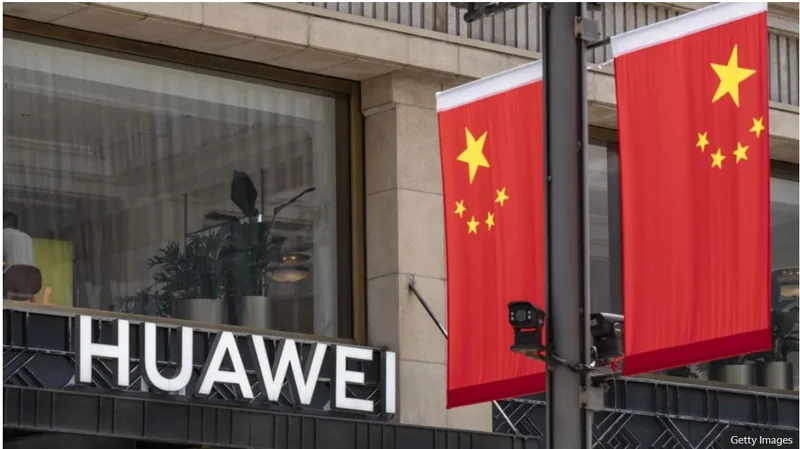
Huawei Technologies has announced a bold strategic goal to achieve transistor density equivalent to 1.4-nanometer processes within the next five years. This ambitious target, revealed at a semiconductor symposium in Shanghai, represents a significant escalation in China’s efforts to achieve technological self-sufficiency in the face of ongoing U.S. trade sanctions. By aiming for the 1.4-nm milestone, Huawei seeks to align its capabilities with global industry leaders such as TSMC, which expects to reach similar manufacturing standards by 2028. This move signals the company’s resilience and its determination to lead the next generation of semiconductor innovation despite severe restrictions on its access to advanced Western manufacturing tools.
To navigate the limitations imposed by sanctions, Huawei is pivoting its focus toward innovative architectural designs rather than relying solely on the traditional method of shrinking transistor sizes. Central to this strategy is the introduction of the "Tau Scaling Law," a principle that emphasizes enhancing chip performance through optimized signal and data movement. Alongside this, the company unveiled a new architecture known as "LogicFolding," designed to improve wiring efficiency and overall processing power. Over the past six years, Huawei has designed 381 different chips, and its upcoming Kirin series will incorporate these new design principles to maintain a competitive edge in both the smartphone and AI sectors.
The announcement follows the successful launch of Huawei’s Mate 60 series, which surprised the global market by utilizing 7-nm technology produced by Semiconductor Manufacturing International Corp (SMIC). This success has bolstered investor confidence, reflected in the positive movement of SMIC’s shares following the Shanghai symposium. Furthermore, Huawei’s Ascend chips are increasingly filling the void left by restricted U.S. technologies in the Chinese AI market. Industry leaders, including the CEO of Nvidia, have acknowledged that the domestic AI landscape in China is becoming increasingly competitive, with Huawei providing a viable alternative for firms unable to access high-end American GPUs.
While industry analysts maintain that China still trails behind the world’s most advanced semiconductor fabricators, Huawei’s roadmap suggests a closing gap. The push for 1.4-nm density is more than a technical objective; it is a critical component of China’s broader geopolitical and economic positioning. As the company prepares to launch its next generation of Kirin chips later this year, the global tech industry is watching closely to see if architectural innovation can truly compensate for the lack of state-of-the-art lithography equipment. Huawei’s progress underscores a shifting dynamic where technological isolation is driving a localized, highly specialized innovation cycle in the heart of the world’s largest electronics market.
This story touches markets covered on Anansi Intelligence ↗.
More from technology
Continue exploring similar stories


